Because of the very cheap ACS712 Current Sensor Board modules available all over the place, I really think that everybody heard about ACS712 sensor from Allegro MicroSystems.
As I was asked if “Can be used as a current sensor module for our ESP8266 Projects without too much hustle?”, I ordered few of them and let’s explore them for the answer 🙂
The ACS712 device consists of a precise, low-offset, linear Hall circuit with a copper conduction path located near the surface of the die. That means that it is a isolated path device, a very nice thing if you want to monitor MAINS Current or any other High Voltage path that you want isolated from your device.
IMPORTANT NOTE !! This device is a Hall Effect transducer. It should not be used near significant magnetic fields. If you have a magnetic noisy environment take a look at other solutions like isolation transformers, isolation OpAmps, linear isolation circuit, bus path isolation, etc.
Theory of operation
Applied current flowing through the ACS712 copper conduction path generates a magnetic field which the Hall IC converts into a proportional voltage. Device accuracy is optimized through the close proximity of the magnetic signal to the Hall transducer.
A precise, proportional voltage is provided by the low-offset, chopper-stabilized BiCMOS Hall IC, which is programmed for accuracy after packaging.
The ACS712 outputs an analog signal, VIOUT that varies linearly with the uni- or bi-directional AC or DC primary sampled current, IP (between IP+ e IP-) within the range specified.
It requires a power supply of 5V (VCC) and two capacitors to filter power supply and output.
CF is recommended for noise management, with values that depend on the application.
Typical application from the Datasheet:
ACS712 Current Board comes in 3 different models of this integrated circuit, depending on the maximum measured current : 5A 20 or 30A
| 5A Module | 20A Module | 30A Module | |
|---|---|---|---|
| Supply Voltage (VCC) | 5VDC | 5VDC | 5VDC |
| Measurement Range | -5 to +5 A | -20 to +20 A | -30 to +30 A |
| Voltage at 0A | VCC/2 | VCC/2 | VCC/2 |
| Scale Factor | 185 mV/A | 100 mV/A | 66 mV/A |
| Variant | ACS712ELC-05A | ACS712ELC-10A | ACS712ELC-30A |
What we will need:
- ACS712 Current Board module (pick your desired choice – 5A, 20A, 30A )
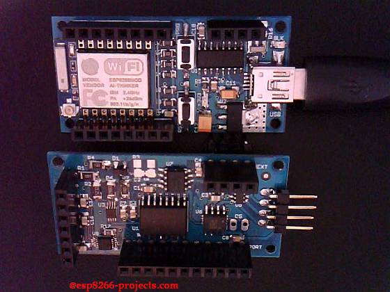
- CBDB Board ( or any other ESP8266 Board you may like but who has the same capabilities)
- USB adapter (take a look on Part 1 for details about the USB Adapter
- 2 x 10 Ω /10 W – Load resistors
- Connection wires – various colors
- Breadboard
- Bench Power Supply
- Voltage Level Shifter and dc amplifier module – VLSAM DC(see details below)
Voltage Level Shifter and amplifier module – VLSAM DC
As our main goal is to explore the posibility to use the ACS712 module with ESP8266 devices, from the description above and datasheet we can identify very quick some problems that need to be solved to make ACS712 a “ESP Friendly” device:
ASC712:
- 5 Vdc power supply device
- measure positive and negative 5/20/30Amps, corresponding to the analog output 100mV/A BUT
- “ZERO” point, means no test current through the output voltage is VCC / 2 =5v/2=2.5V !
ESP8266:
- 3V only device
- ADC range max: 0-1V
What we will need is to “move” the “ZERO” point as low as we want to GND and in the same time to amplify the received analog signal to obtain a better resolution in the desired measuring range. (don’t forget, for our experiment we have DC only voltage here and just one current flow direction)
So, what can be done?
Probably they are some other solutions to this problem, and if you know any of them, please feel free to share in the comments below, but the clasical one is to use a difference amplifier:
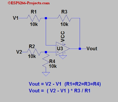
This kind of amplifier uses both inverting and non-inverting inputs of a OPAmp with a gain of one to produce an output equal to the difference between the inputs. Actually if you take a closer look it is a special case of the differential amplifier.
The good thing is that in the same time you can also choose the resistances values in a way to amplify the difference.
If all the resistor values are equal, this amplifier will have a differential voltage gain of 1. The analysis of this circuit is essentially the same as that of an inverting amplifier, except that the noninverting input (+) of the op-amp is at a voltage equal to a fraction of V2, rather than being connected directly to ground. As would stand to reason, V2 functions as the noninverting input and V1 functions as the inverting input of the final amplifier circuit. Therefore:
If we want to provide a differential gain of anything other than 1, we would have to adjust the resistances in both upper and lower voltage dividers, necessitating multiple resistor changes and balancing between the two dividers for symmetrical operation.
A limitation of this simple amplifier design is the fact that its input impedances are rather low compared to that of some other op-amp configurations, most notably the noninverting (single-ended input) amplifier. Each input voltage source has to drive current through a resistance, which constitutes far less impedance than the bare input of an op-amp alone. It is a solution to this problem, fortunately, quite simple, all we need to do is “buffer” each input voltage signal through a voltage follower.
For our case, as we want to “substract” the ACS712 – 2.5Vdc to move the “ZERO” point near GND, we will have:
- V1 = 2.5V – can be easy obtained from 5V with a buffered voltage divider
- V2 = VIOUT – output voltage from ASC712 Module
- Amplification:
- IF R1=R2=R3=R4=10K
- output for ADC input of 100mV/A
- max range: 10A
- resolution: 10mA
- Changing range R1=R2=10K, R3=R4=100k
- output for ADC input of 1V/A
- max range: 1A
- resolution: 1mA
- IF R1=R2=R3=R4=10K
 |
| VLSAM DC Schematic |
And the simulation result for a 0-10A, 2.5-3.5 VIOut sweep:
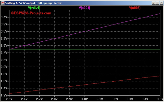 |
- GREEN – Voltage divider output : 2.5Vdc
- FUCHSIA – ASC712 VIOut : 2.5 -> 3.5Vdc
- RED – ADC input : 0 -> 1Vdc


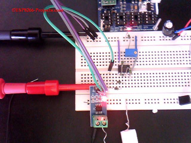

1 Comment
Michaela · August 28, 2018 at 11:06 pm
I was wondering if there would be an easier method to just deliver HIGH on current flowing and low if no current flows. It might be interesting to know how much current is flowing, but for say .. slave devices .. it would be enough to know that some power is being used.So pretty much everything above ZERO point triggers a HIGH, everything at or below ZERO point triggers a LOW. I understand that polarity becomes an issue, but if hard wired, that shouldn’t be a problem.